The Electron Microscopy Facility (EMF) at San Francisco State University houses a Carl Zeiss Ultra 55 Field-Emission Scanning Electron Microscope (FE-SEM). The facility director provides SFSU faculty and students with images and microanalysis of naturally-occurring and fabricated nano-structures across a broad range of disciplines. SFSU researchers are warmly encouraged to contact the facility director for further information regarding microscopy services and how the EMF can provide support for classes through live demonstrations.
Carl Zeiss Ultra 55 (FE-SEM)
The Carl Zeiss Ultra 55 Field Emission Scanning Electron Microscope (FE-SEM) detectors include a chamber-mounted Everhart-Thornley detector (collects secondary and backscattered electrons), an in-lens SE detector (collects high-resolution pure secondary electrons); an on-axis Energy selective Backscattered electron detector (EsB®) (collects energy-filtered backscattered electrons), a Scanning Transmission Electron Detector (STEM); and an Energy Dispersive X-ray Spectrometer (EDS) from Oxford Instruments for chemical analysis of elements from lithium to uranium.
Full Suite of Preparation Equipment
There is a full suite of preparation equipment available in the microscopy facility. SFSU researchers should refer refer to the list of Frequently Asked Questions (FAQs). Consumables specifically designed for the Zeiss SEM are available from several electron microscope accessory vendors, and a list of consumables from one local vendor is provided for convenience.
See the Preparation Equipment
Services
Operation: The facility director operates the FE-SEM for all SFSU researchers as a service, with the goal of providing the highest-quality data in a rapid and cost-effective manner. The extremely bright field-emission electron source and aberration-corrected optics permits ultra-low voltage imaging with nanometer-scale resolution. Researchers within all Departments of the College make use of the electron microscopy facility.
Contact:
Clive Hayzelden, D.Phil.
Email: cliveh@sfsu.edu
Clive Hayzelden, D.Phil.
Clive began using scanning and transmission electron microscopes as an undergraduate, and was instantly hooked. He then studied electron microscopy and microanalysis at Oxford University where he worked on in situ studies of phase transformations in steels using both one-million-volt transmission electron microscopes in the United Kingdom (one at Oxford University for low temperature studies, and one at Imperial College, London, for high temperature studies).
Clive then joined the faculty of Harvard University to build a modern electron microscopy facility, where he taught microscopy techniques to over 620 students over a ten-year period. Clive's research interests have included ultra-high strength steels at Harvard, and in situ atomic resolution imaging of low temperature silicide-mediated crystallization of amorphous silicon at IBM.
Clive has operated Zeiss FE-SEMs since 1995, with the introduction of the first Carl Zeiss DSM 982. He has provided instruction on more than fifty Zeiss FE-SEMs across the United States and Europe. The Zeiss FE-SEM uses an extremely bright electron source, has aberration corrected optics and is designed for ultra-low voltage imaging with nanometer scale resolution.
Contact:
Clive Hayzelden, D.Phil.
Email: cliveh@sfsu.edu
A selection of electron micrographs from research at SFSU
We invite you to peruse the collection of electron micrographs below.
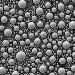
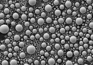
Electron microscopy of materials
Electron micrographs of a range nanostructured materials
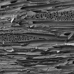
The interior structure of woody plants
Electron micrographs of the cross-sections of a selection of woody plants
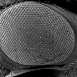
Research into the genetic causes of blindness
Electron micrographs of healthy compound eyes found in wild-type Drosophila melanogaster